Thursday, December 3, 2015

Monitoring TLPs

So far; so good. I implemented the first part of my TLP master plan. The test that I ran is rather simple: I have a version of the titan_wiggle FPGA project with the Lattice's Reveal logic analyzer installed and connected to the PCIe core's receive TLP interface (Fig 1). Titan is installed in a PC running Linux and Shaun's pyhwtest utility.
Figure 1. Block Diagram of the Titan FPGA Design Using Reveal to Capture TLP messages.

pyhwtest is a great little utility. With it I can access the memory space on a PCIe card using python. Everything from simple read/writes to DMA transactions work. With pyhwtest I don't have to write a kernel driver. To use it, all that is required is to find the base address for the BAR that I want to access. Listing 1 (below) shows the output of lspci: BAR0 is mapped to 0xDC000000.


 [root@localhost src]# lspci -d dead:* -v  
 04:00.0 Non-VGA unclassified device: Indigita Corporation Device beef (rev 06)  
     Flags: bus master, fast devsel, latency 0, IRQ 10  
     Memory at dc000000 (32-bit, non-prefetchable) [size=256]  
     Memory at d8000000 (32-bit, non-prefetchable) [size=64M]  
     Capabilities: [50] Power Management version 3  
     Capabilities: [70] MSI: Enable- Count=1/1 Maskable- 64bit+  
     Capabilities: [90] Express Endpoint, MSI 00  
     Capabilities: [100] Device Serial Number 00-00-00-00-00-00-00-00  
 [root@localhost src]#  
Listing 1. Linux Terminal Output Showing the Output from lspci.


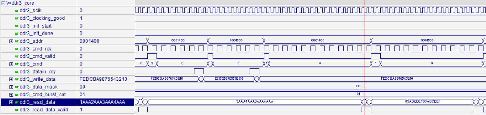
Listing 2 shows the commands required to write 0x12345678 to BAR0 (address 0xDC000000), and Figure 2 shows the Reveal capture that results. It's a good sign that the data written in pyhwtest shows up in the capture. I built a simple spreadsheet to decode the TLP packet (Table 1). From here I'll start thinking about how best to decode the TLP packets in the FPGA and the best way to handle data flow to and from the PC.


 [root@localhost refresh_test]#  
 [root@localhost refresh_test]# python -i titan_test.py -b 0xdc000000  
 Base address: 0xdc000000L  
 >>> hwtest.writelw(BASE, le32_to_be(0x12345678))  
 >>>  
 [root@localhost refresh_test]#  
Listing 2. Python Terminal Output Showing a Data Write to the Base Address of BAR0.


Figure 2. Reveal Capture of the Data Write TLP Message.


H0
RFMTTypeRTCRTDEPAttrRLength
01000000000000000001000000000001
H1
Requester IDTagLast BEFirst BE
00000000000000000000000100001111
H2
AddressR
11011100000000000000000000000000
D0
Data
00010010001101000101011001111000
Table 1. Decode of Captured RX TLP Message.

Wednesday, November 4, 2015

Pushing TLPs

Now that the physical interfaces on Titan have shown to work, the fun part begins. I've given some thought to the firmware framework that Titan needs. In the simplest terms, I want to be able to control and test all of Titan's interfaces from a PC (via PCIe). Developing this firmware will require interfacing to Lattice's PCIe core, the DDR3 core, and a bit of logic glue here and there. I also want to be able to simulate the entire design. A complete simulation environment will allow me to "crack open" the hood and locate bugs much faster than with hardware-only testing.

Lattice's PCIe core presents TLP (transaction layer packets) to the user side of the PCIe core. In past I've used higher level bridges to avoid dealing with TLPs directly. Xilinx has cores available that provide a bus interface to the user (ie. AXI or PLB). Lattice doesn't have a higher level core, but they do have an example of a TLP to Wishbone bridge in the firmware for the ECP3 and ECP5 Versa cards.

While I was tempted to try the TLP to Wishbone bridge, I decided that building firmware to consume TLPs directly had two advantages: It will likely be smaller in the FPGA, and it will give me a chance to understand PCIe transactions better than I have before. How can I pass up a chance to dive a little deeper into PCIe?

The implementation plan is summarized in the Figure 1 block diagram. Then idea is to build two state machines to control the flow of TLP messages between the PCIe core and the registers or FIFOs. One state machine will handle the RX (receive) TLP messages while the second will handle the TX (transmit) messages. The registers will be used for simple interfaces such as the GPIO pins. The FIFOs will handle the buffering and clock domain transition required to interface to DDR3.

Figure 1. Block Diagram of the Titan FPGA Design Connected to a PC.

To simulate the PCIe core, I'm building a testbench where a second PCIe core is instantiated as a stand-in for the PC. I got the idea to connect two PCIe cores together from the Lattice PCIe Endpoint User's Guide. Using a core to test itself would be a bad idea if I was designing the PCIe core itself. Since I'm just implementing a user-side interface, I'm OK trusting that Lattice meets the PCIe SIG standards. Initially this will allow me to write some simple state machines to control the simulation PCIe (Figure 2). Eventually I'll abstract the control interface to the simulation-side PCIe core to allow higher level interface; This will likely be implemented in SystemVerilog, but I'm also considering a python-based interface using MyHDL.


Figure 2. Block Diagram of the Titan FPGA Design Connected to Another PCIe Core Acting as a BFM

So, where to start? I've been reviewing documentation of the structure of TLPs. While TLP isn't overly complex, a complete implementation to handle every possible transaction will take awhile to build. To speed things up a bit I decided to focus my initial work on the most relevant TLPs. My plan is to install Titan in a PC running Linux and use the pyhwtest to send write and read messages. Inside the FPGA, Lattice's Reveal analyzer will be instantiated so I can capture the TLPs received for various commands from Linux. See Figure 3.

I'll use the captured data to design simple synthesizable FSMs (finite state machines) to decode and act on the TLP messages captured in Reveal. Once I have that working, I'll design some simulation FSMs to generate the same messages as the Reveal captured messages. Together, these FSMs will comprise a starting point for the BFM (bus functional model) and Titan simulation of the PCIe link.

Figure 3. Block Diagram of the Titan FPGA Design Using Reveal to Capture TLP messages.

Thursday, October 1, 2015

DesignCon 2016

I purchased my pass for DesignCon 2016 today! Tomorrow is the last day to get the Super Early Bird Special. I'm excited about the trip, and hopefully I'll see some of you out there!

Sunday, September 20, 2015

DDR3 testing

I've been building the simulation environment for Titan lately. For each core that I added to my design, the Lattice tools generate a testbench. I've been working on a unified testbench for Titan that references portions of the Lattice core testbenches. By referencing the Lattice cores test code rather than simply copying them, I can keep my source on GitHub clean.

My initial simulation focus has been on DDR3. I chose DDR3 since it is the last hardware subsystem on Titan that has not been validated. I built a simple state machine that wrote data to two different addresses then read it back. From this simple test it looks like DDR3 is working. Figures 1-6 (below) show the simulation output. Figures 7-9 show the output from the Reveal Logic Analyzer on Titan.

I still need to take some measurements to validate that the signal integrity on the PCB is good, but for now it's good to know that the last subsystem on Titan (DDR3) is functioning.

Figure 1. Write to Address 0x0001400 Marked (Data is 0x1AAA2AAAA3AAA4AAA Followed by 0xE555D555C555B555).

Figure 2. Write to Address 0x0001500 Marked (Data is 0x0123456789ABCDEF Followed by 0xFEDCBA987643210).

Figure 3. Read from 0x0001400 Marked Showing First Word (0x1AAA2AAAA3AAA4AAA).

Figure 4. Read from 0x0001400 Marked Showing Second Word (0xE555D555C555B555).

Figure 5. Read from 0x0001500 Marked Showing First Word (0x0123456789ABCDEF).

Figure 6. Read from 0x0001500 Marked Showing Second Word (0xFEDCBA9876543210).

Figure 7. Overall View Showing DDR3 Test in Hardware (Reveal Analyzer).

Figure 8. Close-Up View Showing DDR3 Data Read from 0x0001400 in Hardware (Reveal Analyzer).

Figure 9. Close-Up View Showing DDR3 Data Read from 0x0001500 in Hardware (Reveal Analyzer).

Thursday, July 16, 2015

Third (and fourth) hand


Am I the only one who gets excited by stuff like this?

Figure 1. Using Hobby Creek's Third Hand to Probe Titan.

Wednesday, July 15, 2015

X-rays and phase shifts

Between taking a trip to see the WNT play in Canada and fighting a persistent bug on Titan, it's been a busy summer.

The initial build and board testing when so well, I was surprised when I started having intermittent problems with the USB JTAG circuit. After looking into USB signal quality, the FT2232H circuit on Titan, and tool issues, I decided that the principle problem was with my PC. I was using Macbook that ran Windows 7 virtually, and a native Windows box seemed more stable.

Unfortunately, when I started to test the SPI flash, I encountered intermittent issues again. The errors varied from failure to identify the SPI flash to intermittent boot failures. While I was at the World Cup, Kevin graciously agreed to debug the problem. He decided to focus on the SPI booting problem exclusively, since it was limited in scope and excluded potential issues with the PC, USB, or JTAG. He confirmed that Titan does not have any power sequencing mistakes and that the part should be booting from flash.

After checking with Lattice, I decided to run another test that validated that the SPI flash was not being accessed too quickly; The SPI flash that I currently have installed cannot be read for 30us after it's VCC (supply voltage) rises to its minimum operating voltage. I probed the SPI flash to monitor the delay between the 3.3V rail going active and the first SPI_CSn (chip select) access. The time before the first SPI access was 16ms which is well outside the 30us requirement.

While monitoring the SPI transactions, I noticed something odd. SPI_CSn and SPI_MOSI were always present, but SPI_CLK was missing at times. This meant that the ECP5 was correctly entering SPI boot mode, and a single signal was the culprit. The only plausible explanation for SPI_CLK disappearing was a connection problem beween the ECP5 and the SPI flash. Since PCBs from PCB-Pool are electrically tested, I began to suspect a solder joint issue. I tried squeezing the ECP5 aganst the PCB and SPI_CLK appeared (Figures 1-3).

I took Titan to a local contract manufacturer and had them X-Ray the ECP5, replace it, and then X-Ray the newly installed part. As Figures 4-5 show, the ECP5 was twisted ever so slightly. I had a similar issue in the past, and I updated my manual reflow profile to prevent it. Apparently I was only preventing gross twisting, but this more subtle twist was a lot harder to detect without an X-Ray.

This demonstrates the problem of working on a new design while also developing a process for prototyping it. I have improvements coming that should eliminate this problem. A colleague is assembling a low volume pick and place machine that I ordered, and I have a controller on the way for my oven. I'll post more about these soon. This was a frustrating problem, but now Titan is almost validated!

Figure 1. Failed SPI Boot.

Figure 2. Failed SPI Boot Attempt with Thumb Pressure on the ECP5.

Figure 3. Successful SPI Boot with Thumb Pressure on the ECP5.

Figure 4. X-Ray Image of the ECP5 IC as Originally Installed.

Figure 5. Close-up of Figure 4 with a PCB Pad Marked in Blue and a BGA Ball in Red.

Figure 6. X-Ray Image of the Newly Installed ECP5.

Thursday, May 7, 2015

C.H.I.P.

I've been very interested in using low cost ARM platforms for my test computers and Linux servers in my home and lab. So far I've got two Raspberry Pi 2 boards as well as a Hummingboard-i2ex from SolidRun. The Hummingboard-i2ex is especially useful for me since it has a PCI Express interface that I need to validate Titan (Figure 1).

Figure 1. Titan and Hummingboard Getting Friendly.

I've never supported a KickStarter project before, but the C.H.I.P. project is a single core ARM board for $9. I thought that a Raspberry Pi was a steal for $35, but the C.H.I.P. is $26 cheaper and it includes flash (eMMC).

Monday, May 4, 2015

PCIe enumeration

Figure 1 doesn't look like much, does it? This simple output from lspci means that the PCI Express interface on the ECP5 is being enumerated on the host. Big step!

Figure 1. Output from lspci

Thursday, April 30, 2015

Rev C bring up

I built the first rev C of Titan earlier this week, and I've been working to bring up the board. This has been the cleanest build yet. It did take about five hours to build by hand, but my process is getting better with each build.

So far I've confirmed that all of the power rails are operational, the on-board USB programming circuit works, and the FPGA can be programmed. The LED counter didn't run when I loaded titan_wiggle, so I'll need to debug a little tonight.

Figure 1. First Rev C.

Tuesday, April 14, 2015

Tuesday, April 7, 2015

Rev C ordered!

Rev C of titan has been released on github, and I ordered the PCB prototypes tonight.

I'm working on an inventory of the components that I have before I order new parts for the build. Thanks to Kevin for a quick review of the PCB.

Figure 1. Rev C of Titan

Saturday, April 4, 2015

A different build


Today a helped a friend, Nick Huskinson, build a PCB board for his senior design project. The board implements a quad ADC using the Linear Tech LTC2170. Since Titan isn't ready yet, Nick designed this board for the Lattice ECP5 development card. Hopefully rev B will have an interface for Titan.

Figure 1. Nick's ADC Board (Ready for Relow).

Figure 2. Nick's ADC Board (After Reflow).

Saturday, March 28, 2015

Rev C almost ready!


I've (finally) completed my changes for rev C of Titan. The token is officially passed to Kevin for review. I'll post more about the changes on this rev soon. For now, enjoy:

Figure 1. Candidate Rev C.

Wednesday, March 25, 2015

DDR3 re-check

I decided to double check the DDR3 routing before finishing rev C of Titan, and I found a few length tuning issues to correct. The updates are committed on github: https://github.com/jsloan256/titan/tree/Rev-C.


Figure 1. Superfluous Picture of Titan's Updated DDR3 Routing.

Friday, March 6, 2015

Expansion interface: looking for problems

Before I dive into final tuning I decided to look for any routing issues with the expansion interface. Figures 1-6 show the issues that I found.  I'm going to shift the routing around a bit to try to limit long runs where traces are run closely in parallel.

Figure 1. Tight Routing Between P3 and P5.

Figure 2. Long Parallel Routing.

Figure 3. Too Tight Length Loop.

Figure 4. Too Tight Length Loop.

Figure 5. Long Parallel Routing.

Figure 6. Too Tight Length Loop and Long Parallel Routing.

Thursday, March 5, 2015

Expansion interface: rough tuning complete

I finally found some cycles to work on Titan today. I was able to complete the rough tuning of the expansion interface. I still need to tune the length a bit more, match the differential pairs, and I have a bit gold plating left (by gold plating I mean adding a little bit of beautification polish). The good news is that I had enough room to match the expansion trace lengths; It was not an easy task with the minimum and maximum trace lengths differing by as much as 2.5 inches.

Figure 1. Rough Tuning Complete.

Thursday, February 12, 2015

Motivation

I let myself get behind on the layout because we didn't know when we would get more ECP5s. Guess what showed up yesterday? Looks like I need to get busy!

Figure 1. The Item.

Wednesday, January 28, 2015

Expansion interface: the tuning begins

I finished connecting all of the expansion nets tonight. The current route is committed on my Titan Github page. The principle trade-off was that I had to use some long traces. Figure 1 shows the current state of the route. I've also listed the minimum and maximum trace lengths for each DDR data group in Table 1. As I start tuning the trace lengths, I may re-route some nets to make the design easier to tune (both by balancing layer usage and shortening the longest routes).

Figure 1. Expansion Route (All Nets Connected, Pre-tuning).

Expansion Header P3Expansion Header P5
A_DQ0 min1239.646B_DQ0 min1718.488
A_DQ0 max3388.985B_DQ0 max2966.341
A_DQ1 min1059.547B_DQ1 min1248.02
A_DQ1 max1604.663B_DQ1 max3499.98
Table 1. Net Minimum and Maximums.


Friday, January 23, 2015

Expansion interface: the depature

My attempts to adjust the expansion header routing by changing pin assignments minimally to make the two headers pinout compatible has turned into an unbounded problem. I decided to change tack. I wiped the current routing, assigned the nets manually, and defined a few groupings to direct the routing.

Within each group I've allowed myself varying level of routing flexibility depending on how critical the net locations are. So far it is going well, hopefully I'll have time to complete the routing this weekend analyze the results. A summary of the working groupings are listed below in priority order:

DQ Group 0 & 1   Each expansion header is connected to a bank that contains two DSQ groups. One of these DQ groups contains the PCLK inputs for the bank as well as the VREF net; This DQS is designated as DQ0 and routed to the long side of the expansion header

PCLK, DQS0, & DQS1   The PCLK input and data strobe (DQ0 & DQ1) differential pairs are assigned to fixed locations that cannot be changed. These nets are routed first and are only allowed layer transitions at the ECP5 and at the expansion header (never more than two). Figure 1 shows my initial route of these nets.

DQ0 pairs 0 & 1 / DQ1 pairs 0 & 1   The first two data pairs adjacent to the data strobes must be "true LVDS TX" pairs from the ECP5 (identified as A/B pairs). They are labeled DQ0-0, DQ0-1, DQ1-0, and DQ1-1. Any A/B pair from the same DQ group may be used. I was able to route these pairs only using vias at the ECP5 and/or the expansion header, like the highest priority pairs (see Figure 2). I'm not sure if we should allow more or not, but since the routing went well I don't have to worry about that today.

DQ0 pairs 2, 3, & 4   The last three differential pairs for each data group (DQ0-2, DQ0-3, DQ0-4, DQ1-2, DQ1-3, DQ1-4) are all routed to ECP5 C/D pairs. Each set of three pairs within the same DQ group (ie. DQ0-2, DQ0-3, & DQ0-4) may be switched to each routing. I have not yet routed these pairs on Titan, but from my examination of the current state of the route (Figure 2) I've concluded that I will have to allow additional via transitions to route all of these pairs (hopefully no more than one additional via).

VREF & D0   The final two nets in the DQ0 data group will be routed as single ended nets (not differential). This is because the VREF net is on a diff pair true net on one bank and on a compliment net on the other bank. There is no common routing that will allow these nets to be differential and have the VREF pin on the same expansion header pin.

D1, D2, D3, & D4   Since the DQ1 data group does not contain a PCLK input or VREF, it has four "extra" nets to route. These will all be routed as singled ended nets.

Figure 1. Top Priority Nets Routed.

Figure 2. Second Priority Nets Routed.

Tuesday, January 6, 2015

Expansion interface: the re-route

Over the holiday I've been considering how painful it will be to re-route the expansions headers on Titan to meet (or approximate) the rules that I defined last week. The answer: Really, really, painful.

The current route is layer efficient and has very few layer transitions (both fantastic qualities). Unfortunately, this natural matching of an ECP5 bank to an expansion connector places DQ groups/strobes, PCLK inputs, and the VREF all over the place. Table 1 shows my analysis of the pinout comparison between expansion headers P3 and P5. I realize that this table is a little busy, but I was trying to look at several different factors at the same time. I considered posting the color version, but it is a rather terrifying to behold.

P5 FunctionP3 FunctionP3 FunctionP5 Function
DQPairOthDQPairOthTop Side NetPin #Bottom Side NetDQPairOthDQPairOth
3.3V21V_I/O
3.3V43V_I/O
GND65GND
89C41CPCLKD0_P (S0)87D8_P (S16)41A89A
89D41DPCLKD0_N (S1)109D8_N (S17)41B89B
GND1211GND
89A41ADQSD1_P (S2)1413D9_P (S18)41C89C
89B41BDQSD1_N (S3)1615D9_N (S19)41D89D
GND1817GND
89A17ADQSD2_P (S4)2019D10_P (S20)17A89ADQS
89B17BDQSD2_N (S5)2221D10_N (S21)17B89BDQS
GND2423GND
53CPCLK41CD3_P (S6)2625D11_P (S22)17C89C
53DPCLK41DD3_N (S7)2827D11_P (S22)17D89D
GND3029GND
GND3231GND
53C41AD4_P (S8)3433D12_P (S24)17C53C
53D41BD4_N (S9)3635D12_N (S25)17D53D
GND3837GND
53C17AD5_P (S10)4039D13_P (S26)17C89C
53D17BD5_N (S11)4241D13_N (S27)17D89D
GND4443GND
53A41CVREFD6_P (S12)4645D14_P (S28)17A53A
53B41DD6_N (S13)4847D14_N (S29)17B53B
GND5049GND
53ADQS41AD7_P (S14)5251D15_P (S30)17C53A
53BDQS41BD7_N (S15)5453D15_N (S31)17D53BVREF
GND5655GND
n/c5857n/c
n/c6059n/c
Table 1. P3 & P5 Pin Mappings.

Figures 1 and 2 show the scale of the problem. Figure 2 especially shows just how clean the current route is. I spent quite awhile looking at different pinouts where where only the most critical nets were routed to the same connector pin. The scale of the change quickly becomes so severe that it doesn't look possible without adding quite a few layer transitions (bad for signal quality) and possibly using more PCB layers (bad for PCB cost).

Figure 1. The Spaghetti Monster.

Figure 2. Routing Layers for the Expansion Interface.

I only have one knob left to twist: function. I have a hunch that only routing about half of the nets as differential pairs will make it much easier to route the rest as single-ended nets. I have a few use-cases in mind. Hopefully I'll find a way to map them to a rational pin mapping.

Reading this you might wonder why I'm taking so much time with this re-planning of the expansion interface. The first is simple: I believe that an intelligent pin assignment will ease the design of modules. The second is all in the schedule: We have our first order of ECP5 FPGA's on the way, but the lead time is long enough for us to give a careful review of the entire design before placing our next PCB order. We intentionally side-stepped the tricky problem of the expansion header design in our first two PCB revs. Now that the rest of the design is stable (or nearly stable), it's time to reconsider this part of the design.