Showing posts with label Lattice. Show all posts

Thursday, December 3, 2015

Monitoring TLPs

So far; so good. I implemented the first part of my TLP master plan. The test that I ran is rather simple: I have a version of the titan_wiggle FPGA project with the Lattice's Reveal logic analyzer installed and connected to the PCIe core's receive TLP interface (Fig 1). Titan is installed in a PC running Linux and Shaun's pyhwtest utility.
Figure 1. Block Diagram of the Titan FPGA Design Using Reveal to Capture TLP messages.

pyhwtest is a great little utility. With it I can access the memory space on a PCIe card using python. Everything from simple read/writes to DMA transactions work. With pyhwtest I don't have to write a kernel driver. To use it, all that is required is to find the base address for the BAR that I want to access. Listing 1 (below) shows the output of lspci: BAR0 is mapped to 0xDC000000.


 [root@localhost src]# lspci -d dead:* -v  
 04:00.0 Non-VGA unclassified device: Indigita Corporation Device beef (rev 06)  
     Flags: bus master, fast devsel, latency 0, IRQ 10  
     Memory at dc000000 (32-bit, non-prefetchable) [size=256]  
     Memory at d8000000 (32-bit, non-prefetchable) [size=64M]  
     Capabilities: [50] Power Management version 3  
     Capabilities: [70] MSI: Enable- Count=1/1 Maskable- 64bit+  
     Capabilities: [90] Express Endpoint, MSI 00  
     Capabilities: [100] Device Serial Number 00-00-00-00-00-00-00-00  
 [root@localhost src]#  
Listing 1. Linux Terminal Output Showing the Output from lspci.


Listing 2 shows the commands required to write 0x12345678 to BAR0 (address 0xDC000000), and Figure 2 shows the Reveal capture that results. It's a good sign that the data written in pyhwtest shows up in the capture. I built a simple spreadsheet to decode the TLP packet (Table 1). From here I'll start thinking about how best to decode the TLP packets in the FPGA and the best way to handle data flow to and from the PC.


 [root@localhost refresh_test]#  
 [root@localhost refresh_test]# python -i titan_test.py -b 0xdc000000  
 Base address: 0xdc000000L  
 >>> hwtest.writelw(BASE, le32_to_be(0x12345678))  
 >>>  
 [root@localhost refresh_test]#  
Listing 2. Python Terminal Output Showing a Data Write to the Base Address of BAR0.


Figure 2. Reveal Capture of the Data Write TLP Message.


H0
RFMTTypeRTCRTDEPAttrRLength
01000000000000000001000000000001
H1
Requester IDTagLast BEFirst BE
00000000000000000000000100001111
H2
AddressR
11011100000000000000000000000000
D0
Data
00010010001101000101011001111000
Table 1. Decode of Captured RX TLP Message.

Wednesday, November 4, 2015

Pushing TLPs

Now that the physical interfaces on Titan have shown to work, the fun part begins. I've given some thought to the firmware framework that Titan needs. In the simplest terms, I want to be able to control and test all of Titan's interfaces from a PC (via PCIe). Developing this firmware will require interfacing to Lattice's PCIe core, the DDR3 core, and a bit of logic glue here and there. I also want to be able to simulate the entire design. A complete simulation environment will allow me to "crack open" the hood and locate bugs much faster than with hardware-only testing.

Lattice's PCIe core presents TLP (transaction layer packets) to the user side of the PCIe core. In past I've used higher level bridges to avoid dealing with TLPs directly. Xilinx has cores available that provide a bus interface to the user (ie. AXI or PLB). Lattice doesn't have a higher level core, but they do have an example of a TLP to Wishbone bridge in the firmware for the ECP3 and ECP5 Versa cards.

While I was tempted to try the TLP to Wishbone bridge, I decided that building firmware to consume TLPs directly had two advantages: It will likely be smaller in the FPGA, and it will give me a chance to understand PCIe transactions better than I have before. How can I pass up a chance to dive a little deeper into PCIe?

The implementation plan is summarized in the Figure 1 block diagram. Then idea is to build two state machines to control the flow of TLP messages between the PCIe core and the registers or FIFOs. One state machine will handle the RX (receive) TLP messages while the second will handle the TX (transmit) messages. The registers will be used for simple interfaces such as the GPIO pins. The FIFOs will handle the buffering and clock domain transition required to interface to DDR3.

Figure 1. Block Diagram of the Titan FPGA Design Connected to a PC.

To simulate the PCIe core, I'm building a testbench where a second PCIe core is instantiated as a stand-in for the PC. I got the idea to connect two PCIe cores together from the Lattice PCIe Endpoint User's Guide. Using a core to test itself would be a bad idea if I was designing the PCIe core itself. Since I'm just implementing a user-side interface, I'm OK trusting that Lattice meets the PCIe SIG standards. Initially this will allow me to write some simple state machines to control the simulation PCIe (Figure 2). Eventually I'll abstract the control interface to the simulation-side PCIe core to allow higher level interface; This will likely be implemented in SystemVerilog, but I'm also considering a python-based interface using MyHDL.


Figure 2. Block Diagram of the Titan FPGA Design Connected to Another PCIe Core Acting as a BFM

So, where to start? I've been reviewing documentation of the structure of TLPs. While TLP isn't overly complex, a complete implementation to handle every possible transaction will take awhile to build. To speed things up a bit I decided to focus my initial work on the most relevant TLPs. My plan is to install Titan in a PC running Linux and use the pyhwtest to send write and read messages. Inside the FPGA, Lattice's Reveal analyzer will be instantiated so I can capture the TLPs received for various commands from Linux. See Figure 3.

I'll use the captured data to design simple synthesizable FSMs (finite state machines) to decode and act on the TLP messages captured in Reveal. Once I have that working, I'll design some simulation FSMs to generate the same messages as the Reveal captured messages. Together, these FSMs will comprise a starting point for the BFM (bus functional model) and Titan simulation of the PCIe link.

Figure 3. Block Diagram of the Titan FPGA Design Using Reveal to Capture TLP messages.

Sunday, September 20, 2015

DDR3 testing

I've been building the simulation environment for Titan lately. For each core that I added to my design, the Lattice tools generate a testbench. I've been working on a unified testbench for Titan that references portions of the Lattice core testbenches. By referencing the Lattice cores test code rather than simply copying them, I can keep my source on GitHub clean.

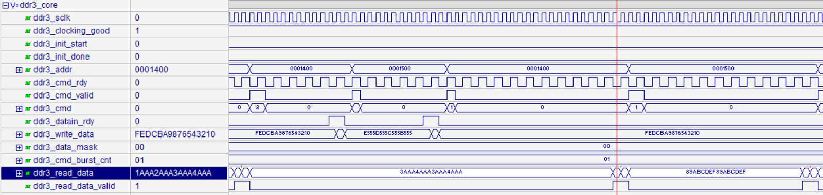
My initial simulation focus has been on DDR3. I chose DDR3 since it is the last hardware subsystem on Titan that has not been validated. I built a simple state machine that wrote data to two different addresses then read it back. From this simple test it looks like DDR3 is working. Figures 1-6 (below) show the simulation output. Figures 7-9 show the output from the Reveal Logic Analyzer on Titan.

I still need to take some measurements to validate that the signal integrity on the PCB is good, but for now it's good to know that the last subsystem on Titan (DDR3) is functioning.

Figure 1. Write to Address 0x0001400 Marked (Data is 0x1AAA2AAAA3AAA4AAA Followed by 0xE555D555C555B555).

Figure 2. Write to Address 0x0001500 Marked (Data is 0x0123456789ABCDEF Followed by 0xFEDCBA987643210).

Figure 3. Read from 0x0001400 Marked Showing First Word (0x1AAA2AAAA3AAA4AAA).

Figure 4. Read from 0x0001400 Marked Showing Second Word (0xE555D555C555B555).

Figure 5. Read from 0x0001500 Marked Showing First Word (0x0123456789ABCDEF).

Figure 6. Read from 0x0001500 Marked Showing Second Word (0xFEDCBA9876543210).

Figure 7. Overall View Showing DDR3 Test in Hardware (Reveal Analyzer).

Figure 8. Close-Up View Showing DDR3 Data Read from 0x0001400 in Hardware (Reveal Analyzer).

Figure 9. Close-Up View Showing DDR3 Data Read from 0x0001500 in Hardware (Reveal Analyzer).

Tuesday, April 7, 2015

Rev C ordered!

Rev C of titan has been released on github, and I ordered the PCB prototypes tonight.

I'm working on an inventory of the components that I have before I order new parts for the build. Thanks to Kevin for a quick review of the PCB.

Figure 1. Rev C of Titan

Friday, January 23, 2015

Expansion interface: the depature

My attempts to adjust the expansion header routing by changing pin assignments minimally to make the two headers pinout compatible has turned into an unbounded problem. I decided to change tack. I wiped the current routing, assigned the nets manually, and defined a few groupings to direct the routing.

Within each group I've allowed myself varying level of routing flexibility depending on how critical the net locations are. So far it is going well, hopefully I'll have time to complete the routing this weekend analyze the results. A summary of the working groupings are listed below in priority order:

DQ Group 0 & 1   Each expansion header is connected to a bank that contains two DSQ groups. One of these DQ groups contains the PCLK inputs for the bank as well as the VREF net; This DQS is designated as DQ0 and routed to the long side of the expansion header

PCLK, DQS0, & DQS1   The PCLK input and data strobe (DQ0 & DQ1) differential pairs are assigned to fixed locations that cannot be changed. These nets are routed first and are only allowed layer transitions at the ECP5 and at the expansion header (never more than two). Figure 1 shows my initial route of these nets.

DQ0 pairs 0 & 1 / DQ1 pairs 0 & 1   The first two data pairs adjacent to the data strobes must be "true LVDS TX" pairs from the ECP5 (identified as A/B pairs). They are labeled DQ0-0, DQ0-1, DQ1-0, and DQ1-1. Any A/B pair from the same DQ group may be used. I was able to route these pairs only using vias at the ECP5 and/or the expansion header, like the highest priority pairs (see Figure 2). I'm not sure if we should allow more or not, but since the routing went well I don't have to worry about that today.

DQ0 pairs 2, 3, & 4   The last three differential pairs for each data group (DQ0-2, DQ0-3, DQ0-4, DQ1-2, DQ1-3, DQ1-4) are all routed to ECP5 C/D pairs. Each set of three pairs within the same DQ group (ie. DQ0-2, DQ0-3, & DQ0-4) may be switched to each routing. I have not yet routed these pairs on Titan, but from my examination of the current state of the route (Figure 2) I've concluded that I will have to allow additional via transitions to route all of these pairs (hopefully no more than one additional via).

VREF & D0   The final two nets in the DQ0 data group will be routed as single ended nets (not differential). This is because the VREF net is on a diff pair true net on one bank and on a compliment net on the other bank. There is no common routing that will allow these nets to be differential and have the VREF pin on the same expansion header pin.

D1, D2, D3, & D4   Since the DQ1 data group does not contain a PCLK input or VREF, it has four "extra" nets to route. These will all be routed as singled ended nets.

Figure 1. Top Priority Nets Routed.

Figure 2. Second Priority Nets Routed.

Monday, December 29, 2014

Expansion interface: rules

Before Christmas Kevin and I discussed the expansion header rule-set that I posted last time. I ended up giving him a little clarification. What follows is a summary. Keep in mind that this is a work in progress. Once we finish the new expansion routing for rev C we will post a summary and use case examples.

Figure 1. A View of the MEC8-RA Expansion Header on Titan.


Trace Lengths and Matching All signal trace lengths must be matched to within 20mils and may not exceed 2000mils. Additionally each differential pair in the bank will be routed as a differential pair each pair's N and P net will be length tuned within 5mils. This tuning is intentionally over-kill to reserve as much margin as possible for the routing on modules.

TX and RX pair assignments All LVDS transmit pairs must be connected to the same side of the expansion connector. Figure 2 shows and mapping that meets this rule. This rule is included because the Samtec MEC8-RA connector as longer pins on one side of the connector. Figure 3 was taken from the MEC8-RA's STEP file. My rough measurements show that the top pins are about 100mils longer than the bottom pins. We can avoid accounting for this difference by routing the ECP5's true LVDS transmitter pairs on one side (labelled as pads A and B) and the receiver pairs (labelled as pads C and D) on the other side.

Figure 2. An TX/RX Mapping Example (TX on the Long Side, RX on the Short Side).

Figure 3. A Top and Bottom Pin Pair from the MEC8-RA.

DQ Pin assignments Each DQ group must be matched to the same set of diff pairs; Within the each DQ group the DQS pair must be on a fixed pin. Figure 4 shows an example DQ mapping. This rule means that the individual DQ pair assignments are not fixed and may be routed differently to ease routing.

Figure 4. An Example Mapping of the Two DQ Groups from an ECP5 Bank.

Other Fixed Pin Assignments The bank's VREF net and PCLK on C/D pads must be routed to fixed pins.


Friday, December 19, 2014

Expansion interface

We are finalizing our plans for rev C of Titan now. Over the last week Kevin has been working on our current change list: layout adjustments to ease manufacture, tighter tuning of the expansion header traces, and the addition of a 1.2V power supply for the SerDes (PCIe) transmitter and receiver. Kevin is working in his fork of the Titan project. Once he completes his changes I'm going to make a few adjustments to the DDR3 layout. When we are ready to order we will pull the changes back into the master branch of Titan on the C-E-S organization Github page.

While Kevin is updating the layout, I've been focused on validated our changes. Initially I was working on using the Diamond's Reveal embedded logic analyzer to identify the PCIe issues. Now that I know that there isn't a PCIe core in the samples we have, I'm focusing my efforts on validating the DDR3 memory design and the external interfaces.

Figure 1. Titan Rev B with Two Expansion Modules Installed.

Our expansion headers bring out a single bank of the ECP5 FPGA to a single connector. Now that we've had more time to consider possible expansion modules it has become clearer how we should organize the connections from the FPGA's I/O banks to the connectors. We are trying to balance keeping the layout simple and clean with our desire to standardize the expansion header pinout to make our future modules interchangeable from one Titan header to another.

Each FPGA bank that we have connected to an expansion header can be configured as 32 single-ended GPIOs, 16 differential GPIOs, two DDR data groups, or 7:1 geared interfaces (ie. CameraLink). Lattice's ECP5 High-Speed I/O Interface guide describes the interface possibilities. One specific interface that we are studying that has applications with SDR is the Linear Technology LTC217x quad ADC.

This leads me to my list of features that need to be the same from one expansion header to another. These assignments are based on the expansion differential pair nomenclature used on the rev B Titan schematic (see Figure 2).

Figure 2. Titan Expansion Header (showing our simple nomenclature).

Titan Expansion Header Features

  • One PCLK pair must assigned to a fixed diff pair (ie. DO_P/N)
  • Each of the two DQS pairs must be assigned to a fixed diff pair (ie D8_P/N and D12_P/N)
    • Each DQ group must be matched to the same set of diff pairs (ie D0/1/2/3/9/10/11_P/N)
  • VREF must be assigned to a fixed net (ie. D1_P)
  • All LVDS transmit pairs must be connected to the same side of the expansion connector (ie. D0/1/2/3/4/5/6/7_P/N)
  • All trace lengths must be matched to within 20mils and may not exceed 2000mils.
Now we'll see if I've given Kevin an impossible set of requirements. If I have I'm sure that I'll hear about it.

Thursday, December 18, 2014

Stupid mistakes

Through my career I've had the pleasure of working with some intelligent and talented engineers and scientists. Along the way I've learned to listen when I'm given advice. I might decide not to heed their advice, but I always listen. The two most memorable nuggets of advice that I've received are:
  1. Don't be a candy ass
  2. Don't sweat the stupid mistakes, it's the smart mistakes that should worry you
Tonight I'm trying hard to remind myself of #2. The principle is simple; We all make silly mistakes, overlook things, or just forget something. As long as we identify our mistakes quickly and move on it shouldn't be a problem. The bad mistakes are ones where you focus on something for a long time and come to the wrong conclusion. These smart mistakes often mean that you really don't understand the problem.

While debugging our two rev B boards, we've seen several successes. Our external expansion headers are working, the power rails all work, and the USB programming circuit all work. Unfortunately we were not able to get the PCI Express interface to operate. We found three issues that prevented PCIe from working:
  1. From testing on the Lattice ECP5 PCI Express card, I showed that my implementation would only enumerate the PCIe interface on Diamond 3.2, not 3.3. This isn't too big a deal since I can just go back to 3.2 for now.
  2. We did not include LDOs for the SerDes (PCIe) transmitter and receiver. We were able to repurpose an LDO on Titan to provide the 1.2V as required by the ECP5 SERDES/PCS Usage Guide. This LDO wire-mod can be seen in the LED blinky video (below) on the left side of the ECP5. The mod worked well, and I verified that the noise level at the decoupling caps nearest to the ECP5 was similar to that measured on the Lattice's ECP5 card.
  3. The third issue keeping PCIe from working on Titan can be seen in the blinky video. Watch it again at 720p or higher as see if you can find it. I recommend watching it in full screen.


Did you see it? The engineering samples that we used on the rev B boards were part number LFE5U-85F-8BG381IES. I noticed this when I was building a DDR3 test project tonight. The correct part number is LFE5UM-85F-8BG381IES. What does the M mean? SerDes. We are testing parts without the SerDes (PCIe) interface included.

Wednesday, December 10, 2014

Second build of rev B


As Kevin mentioned yesterday, we were able to build a second rev B Titan using the ECP5 that we reclaimed from our rev A build. I'm still working to get the PCI Express interface to enumerate, but the build went well as the video above shows.

We've found a few clear errors in the PCB that we need to fix and we've already started some preliminary work on rev C. I'll outline what we found as soon as we have a more complete list.

Sunday, November 30, 2014

PCIe enumeration

Today was a day for good news and even better news. I passed the Titan PCBs to Kevin to review our options to get the board up and running, and I focused on the firmware any why the PCIe interface didn't enumerate on the Titan prototype.

Since the titan_wiggle project was a fork from ecp5dev_wiggle, I decided to validate that the Lattice ECP5 PCI Express Card enumerated properly on my test PC; It did not enumerate. I know that ecp5dev_wiggle enumerated in the past, but now I'm wondering if I failed to check PCIe enumeration at every step during development. The last two significant changes were the Diamond update from 3.2 to 3.3 and the pairing down of the project I did before I posted it to Github.

I followed IPUG112_01.2 closely and rebuilt the PCIe core in the Lattice Clarity tool in Diamond 3.3 and the PCIe interface still did not enumerate on the ECP5 dev card. I then rebuilt the project in Diamond 3.2 and the board enumerated properly. That explains why Titan didn't enumerate since it was running a direct fork of ecp5dev_wiggle in Diamond 3.3. I'm going to contact Lattice and see what might be wrong with my 3.3 project, but for now I can test Titan in Diamond 3.2 as soon as we have another working Titan.

On the PCB front, Kevin has been working working on an idea that we have to repair our Titan prototype. When I was last inspecting our rev A prototype the ECP5 popped of the board. Popping off wasn't that surprising since the rev A's pads were so small that we had virtually no ball collapse. Kevin's review of the part showed that we should be able to use it to replace the (possibly) damaged ECP5 on our rev B board. His next step is to isolate the LDOs on shorted rails from the ECP5 to determine if the failure is in the ECP5, the LDOs, or both.

Friday, November 28, 2014

And the sparks fly...

I'm still trying to wrap my head around it, but unfortunately I destroyed our only working Titan prototype while testing it. The build went very well, and I got a lot of good data from testing the card. While Kevin and I consider our next steps, I'll review how we got here.

Building

The rev B board assembly went very smoothly. I simplified the build by not loading the USB programming circuit, and I was able to place and reflow the board myself (including the two BGA parts). The only items that required manual rework after the build were two twisted capacitors and the switching power supply IC in a QFN package at U10. U10 also skewed in the same direction on the rev A build so we are going to examine this issue more deeply later.

Figure 1. U10, Skewed by a Pad.

We decided to simple remove U10 and bypass the 12V to 3.3V power supply and use the PCI Express connector's 3.3V rail instead. With U10 removed, this just required a simple mod-wire.

Testing

Prior to powering the board I measured the impedance to ground on each voltage rail:

RailLocation MeasuredImpedance
3.3VC866 kOhms
2.5V_AC604.8 kOhms
1.1V_AC314.3 kOhms
1.1VC5979 Ohms
2.5VC674.1 kOhms
1.5VC272 kOhms
     Table 1. Impedance Measurements.

RailLocation MeasuredVoltage
3.3VC863.472 V
2.5V_AC602.49 V
1.1V_AC311.099 V
1.1VC591.096 V
2.5VC672.480 V
1.5VC271.499 V
     Table 2. Voltage Measurements.

Using a Lattice USB programmer, I used Diamond to validate that the ECP5 was identified with a JTAG scan. I then loaded my titan-wiggle test project and two LED expansion boards to validate That 64 I/O pins (32 to each expansion header) all work as my video shows.

Next I rebooted the Linux PC that was powering Titan and used the lspci command see if the PCI Express interface enumerated; It did not enumerate. I was able to validate the PERSTn (the PCI Express reset signal) and REFCLK were being received by the FPGA. Titan-wiggle uses PERSTn as its reset; I simply issued a warm reboot (linux reboot command) and saw that the LED counter reset during the PC's reboot. I then changed the LED counter from the 50MHz oscillator to the 125MHz output from the PCIe core and the LED counting pattern speed increased as I expected.

This is when the damage to Titan occurred. The mod-wire bypassing U10 was connected to a 3.3V via very close to the PCIe connector. With Titan installed into the PC and powered I accidentally nudged the board and the mod-wire popped off the via. The wire was under tension and swung across the card, most likely contacting the 12V rail on nearby caps. This would have shorted the ECP5's 3.3V rail directly to 12V. I saw a spark and a little smoke. As we all know, it is nearly impossible to return all of the smoke to an IC once it escapes :p  I powered off the unit and checked the voltage rails and found that the 3.3V, 2.5V, and 1.1V rails were all shorted to ground.

While this is disheartening, mistakes do happen, and hopefully we can recover quickly. For now I will be focusing on firmware development using the Lattice PCIe Development Kit and developing theories about why the PCI Express interface did not enumerate

Tuesday, November 25, 2014

More signs of life

I used two Dione LED boards and the titan_wiggle FPGA project to validate that all of the expansion I/O pins work. Next step, PCIe!

Titan Lives!

All of the power rails on the rev B board come up correctly and the FPGA is detected in Diamond via JTAG!

More details tonight.

Wednesday, November 12, 2014

Test setup

I've been giving some thought to the best development platform for Titan. I'm trying to optimize several criteria at the same time:

  • Low cost
    • While this seems self-evident, I'm not purely interested in cheap. I could always find a cheap PC with a PCI Express (PCIe) slot and use it. I'm looking for an inexpensive platform that also meets my other needs:
  • Repeatability
    • I'd like to find a platform that I can replicate in a hurry. The idea here is for Kevin and I to have similar setups that can be built up quickly and that we can share easily.
  • Accessibility
    • Accessibility is all about sharing. If I can create a common test platform that Kevin and I are both familiar with we will end up spending less time configuring test systems and more time developing HDL and hardware.
  • Future Development Modeling
    • I'm also interested in using test platforms that may model future FPGA/CPU pairings that show promise. This leads me to consider non-Intel platforms.
  • Easy to Use with Linux

Usually I end up using one PC with my UUT (PCIe express card that I'm testing) and another PC with the JTAG programmer and other GUI based development tools. 

For Titan I'm considering moving to an environment where a small, low-cost platform is used to provide the PCIe link to Titan as well as the USB ports for any development tools that I need (JTAG programmer, logic analyzer, etc.). The plan is to use the USB/IP open source project to share the USB ports from the PCIe host platform to a my laptop (or Kevin's) where I can run the GUI based Lattice Diamond or SaleAE logic analyzer software. Figure 1 shows this idea.


Figure 1. Titan Development Configuration Idea.

I'll have to do some testing with USB/IP to see how practical this is, but I'm confident enough that I went ahead and ordered some hardware:
  • SolidRun HummingBoard-i2eX
    • $119.00 with AC power supply and 8GB micro-SD card.
  • Bplus PM2 PCI-E / Mini PCI-E adapter
    • $40. This is a little pricey and seems like a negative at first. I looked for a simple ARM-based processor board few low-cost options had PCIe slots (most had mini-PCIe like the Hummingboard). My long term plan is to build my own mini-PCIe to PCIe adapter with a GPIO input capable of power cycling Titan.

Wednesday, September 3, 2014

Oh, the lights!


My heart grows three sizes every time I see an FPGA make LEDs blink! This simple project has been checked into CES's github account: https://github.com/c-e-s/ecp5dev_wiggle

I will create new repos under the c-e-s organization as I practice building simple projects using Diamond 3.2 for the Lattice ECP5 PCI Express board.

Tuesday, September 2, 2014

DDR3 initial route complete!

I finished routing and tuning the DDR3 circuit last night. My branch of the Titan PCB layout is now in Kevin's hands for re-integration into trunk. I'll post some screen caps of the layout when the integration is complete. My next task will be to build a test project for the Lattice's new ECP5 PCI Express Board. When I get it working I'll port the code to Titan and validate our pinout.

Until then, enjoy our latest post at the CES blog: Lattice's ECP5 PCI Express Card